Record Data Sheet
NVIDIA, AMD and Broadcom are expanding advanced packaging, substrate and interconnect capacity as AI chip manufacturing becomes increasingly capital-intensive. But will the returns justify the investment?
The investment thesis
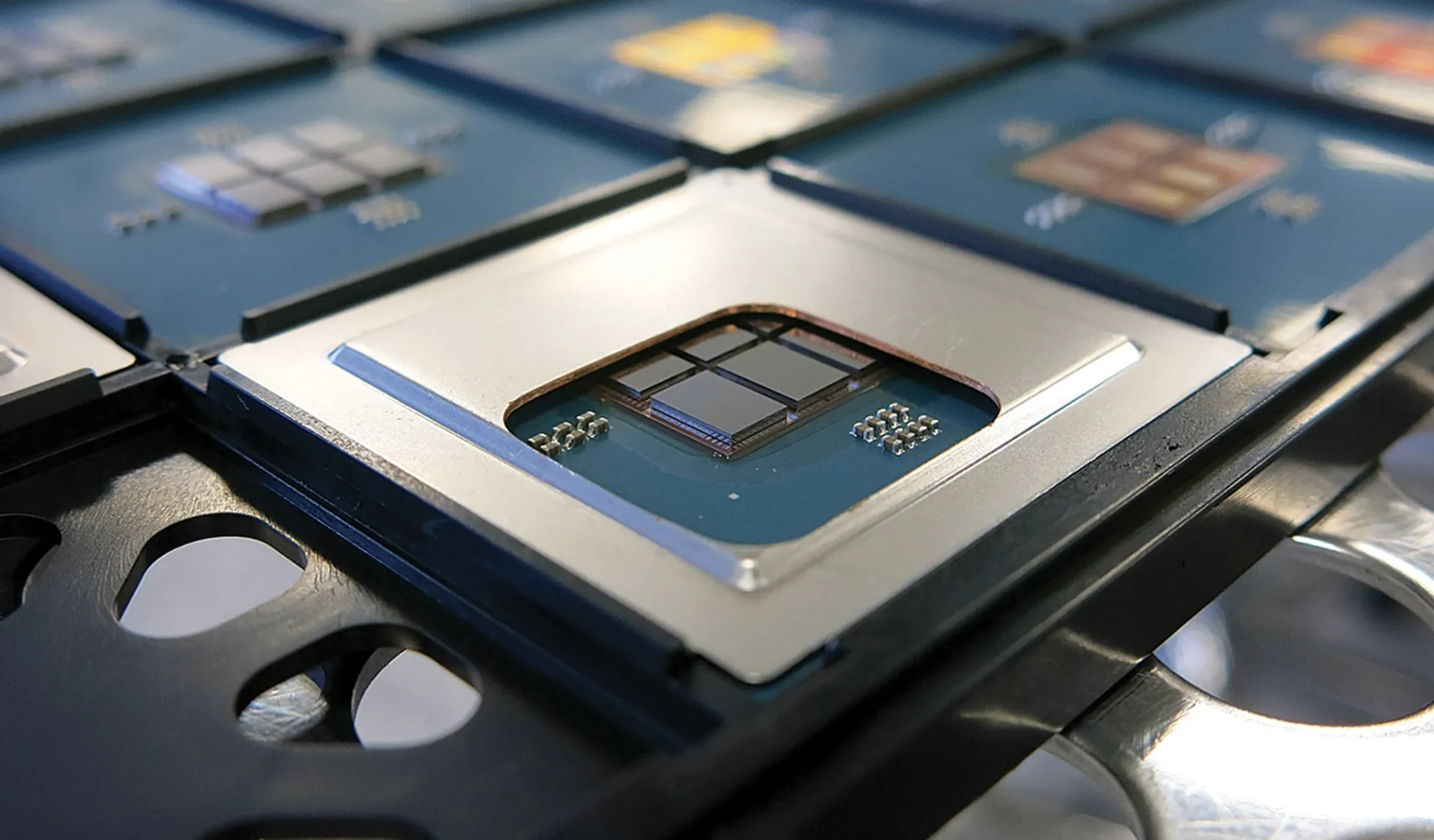
The semiconductor industry’s next capacity constraint may not be the production of smaller transistors. It may be the ability to connect, package, test and deliver increasingly complex chips at commercial scale.
Advanced semiconductor packaging has become strategically important because modern AI accelerators are no longer economically or technically defined by a single processor. They depend on the integration of compute dies, high-bandwidth memory, interconnects and other components into tightly engineered systems. The performance of the final product increasingly depends on how efficiently these components communicate, how much power they consume and how reliably they can be manufactured together.
Yole Group forecasts that global capital expenditure on advanced packaging could approach $28 billion in 2026, according to Reuters. This estimate points to a major expansion in the sector, although it should be treated as an industry forecast rather than a disclosed pool of committed investment. It is not NVIDIA’s spending, AMD’s spending or a combined corporate investment figure.
The strategic shift is already visible. NVIDIA is expanding relationships with packaging, substrate and testing suppliers. AMD has announced more than $10 billion in investment across Taiwan’s semiconductor ecosystem. Broadcom is participating in new substrate and packaging initiatives, while suppliers such as Amkor, ASE, SPIL, Powertech Technology and IBIDEN are positioning themselves for a larger role in the AI supply chain.
For investors, the important question is not simply how much capacity is being announced. It is who will own that capacity, who will finance it, how much of it is secured by customer commitments, and whether the resulting returns will justify the capital employed.
The expansion of advanced packaging capacity is part of a much larger investment cycle in artificial intelligence infrastructure. As discussed in our analysis of Google vs Amazon: AI Infrastructure Spending, the financial commitment extends well beyond GPUs and data centers. It also reaches the manufacturing capacity, components and industrial infrastructure required to bring AI systems into operation.
1. Why advanced packaging is becoming strategically valuable
Advanced packaging combines multiple semiconductor components into a single integrated package. Technologies such as 2.5D and 3D integration allow processors and memory to operate together with shorter interconnections and higher bandwidth than would be practical with conventional approaches.
This matters particularly for AI infrastructure. As accelerator performance increases, data movement between compute and memory becomes a critical determinant of system performance. More processing power alone does not guarantee better economics if the system cannot move data efficiently or if power consumption and thermal constraints limit utilization.
Packaging therefore sits at the intersection of three economic variables:
- Performance: higher bandwidth and more efficient communication between components.
- Power efficiency: reduced energy costs per unit of useful computation.
- Manufacturing economics: the ability to integrate more functionality while maintaining acceptable yields, reliability and production costs.
The third variable is particularly important. A technically successful process is not automatically a commercially attractive one. Complex packaging requires specialized equipment, materials, engineering expertise and process control. Yield losses can quickly erode margins, especially when packages incorporate expensive processors and high-bandwidth memory.
This creates an opportunity for suppliers with established manufacturing capabilities. It also creates a substantial barrier to entry for new competitors.
The competitive position of semiconductor manufacturers is equally important. The relationship between production capacity, memory technology and AI demand is examined further in our analysis of CXMT vs Micron: Memory and AI.
2. NVIDIA: securing capacity across the supply chain
NVIDIA’s October 21, 2026 announcement provides one of the clearest indications of how AI chipmakers are approaching the capacity problem.
The company disclosed expansion agreements with six manufacturing partners: Amkor Technology, IBIDEN, King Yuan Electronics (KYEC), Samsung Electro-Mechanics, Siliconware Precision Industries (SPIL) and Unimicron.
The agreements cover several distinct parts of the supply chain. They should not be treated as one homogeneous advanced-packaging investment.
Amkor Technology — advanced packaging
NVIDIA and Amkor plan to expand advanced packaging capacity, with Amkor targeting an increase of more than 300% in interposer wafer capacity by the end of 2028.
This follows a separate July 2026 announcement of a $1.5 billion multi-year advanced packaging and development agreement. Under that agreement, NVIDIA will provide a prepayment to support the expansion of Amkor’s U.S. advanced packaging capacity.
The distinction matters. The $1.5 billion figure represents the value of the announced agreement, not necessarily Amkor’s independently funded capital expenditure. The prepayment structure also changes the financing profile: NVIDIA helps support capacity expansion while securing access to manufacturing capabilities it considers strategically important.
For Amkor, customer-backed expansion can reduce the risk of investing ahead of demand. However, the ultimate return will depend on production yields, the pace of qualification, operating costs and the volume of business that remains after the initial agreements.
IBIDEN — high-performance package substrates
IBIDEN is investing approximately ¥500 billion in its electronics business over fiscal years 2026–2028 to expand high-performance IC package substrate capacity.
The first disclosed phase includes approximately ¥220 billion for the Gama Plant, with operations and mass production expected to begin progressively from fiscal 2027. The broader investment plan also includes the Ono Plant and other existing facilities.
Substrates are a critical part of advanced semiconductor packages. They provide the electrical and mechanical connections between the silicon components and the wider system. As packages become larger and more complex, substrate specifications become more demanding.
IBIDEN’s investment is strategically relevant to AI infrastructure, but it should not be described as a direct NVIDIA investment. It is a supplier capital expenditure plan designed to serve high-performance computing demand across its customer base.
SPIL — optical engines and co-packaged optics
NVIDIA and SPIL plan to expand manufacturing capacity in Taiwan for optical engines used in co-packaged optics. NVIDIA says SPIL is targeting a 15-fold increase in this capacity by mid-2027, followed by another doubling by the end of 2028.
This is a different technology and investment category from conventional CoWoS packaging. Co-packaged optics brings optical connectivity closer to the computing system, potentially addressing bandwidth, power and interconnect constraints as AI clusters scale.
The distinction is important because it illustrates how the bottleneck may move beyond packaging processors and memory. Connectivity between systems is becoming another area where manufacturing capacity and technical execution can determine the pace of AI infrastructure deployment.
NVIDIA’s announcement confirms the planned SPIL expansion. It does not, by itself, confirm reports that NVIDIA is financing billions of dollars of additional CoWoS capacity at SPIL. That separate financing claim has been reported by Reuters but has not been established in the official NVIDIA announcement.
KYEC — semiconductor testing
NVIDIA also disclosed a $1.1 billion capacity-reservation advance to King Yuan Electronics to support new U.S. testing facilities and equipment. High-volume production is targeted for April 2027.
Testing is essential to the semiconductor production chain, but this figure should not be classified as advanced packaging expenditure. It is a capacity-reservation arrangement supporting semiconductor testing infrastructure.
The broader lesson is that the AI supply chain is being financed across multiple stages, not just at the wafer fabrication or packaging level.
Samsung Electro-Mechanics and Unimicron — substrate capacity
NVIDIA’s agreements with Samsung Electro-Mechanics and Unimicron, alongside IBIDEN, are expected to support a 2.5-fold increase in substrate capacity over three years.
NVIDIA has not disclosed a single combined investment amount for these substrate agreements. Unimicron’s expansion in Taiwan is expected to begin contributing capacity from 2027, with full capacity targeted by mid-2028.
These agreements reinforce the importance of materials and substrate suppliers in the AI infrastructure cycle. They also demonstrate why looking exclusively at GPU manufacturers can overlook important parts of the industry’s capital expenditure chain.
3. AMD: more than $10 billion across Taiwan’s semiconductor ecosystem
AMD announced on May 21, 2026, that it would support more than $10 billion in investments across Taiwan’s semiconductor ecosystem to expand strategic partnerships and advanced packaging capabilities for AI infrastructure.
The figure is significant, but its interpretation requires care. AMD described investment across an ecosystem; it did not present the entire amount as a single direct capital expenditure commitment by AMD or provide a complete project-by-project breakdown.
The announcement identifies several important manufacturing relationships.
ASE and SPIL are collaborating with AMD and other partners on wafer-based 2.5D Elevated Fanout Bridge (EFB) technology. The objective is to improve interconnect bandwidth and power efficiency for next-generation processors.
Powertech Technology (PTI) has qualified what AMD describes as the industry’s first 2.5D panel-based EFB interconnect. Panel-based processing could offer a different manufacturing economics model by enabling larger processing formats and potentially improving material utilization.
AMD also identified Unimicron, Nan Ya PCB and Kinsus as partners in substrate technology.
The ecosystem extends beyond packaging. AMD’s Helios rack-scale platform involves manufacturing partners including Sanmina, Wiwynn, Wistron and Inventec. These companies are relevant to the production and integration of complete AI systems, rather than being interchangeable with semiconductor packaging suppliers.
This distinction matters for capital allocation. The economics of a GPU package, a substrate, a server rack and a complete data-center system are different. Their investment requirements, margins, customer relationships and exposure to the AI cycle should be evaluated separately.
AMD’s strategy is not simply to replicate NVIDIA’s supplier network. It is to develop alternative manufacturing capabilities and a broader ecosystem that can support its own accelerator and rack-scale roadmap.
4. Powertech and Broadcom: the economics of panel-level packaging
One of the more interesting developments is the proposed joint venture between Powertech Technology and Broadcom.
Powertech’s board approved an investment of $400 million in a proposed Singapore joint venture with Broadcom. The project is intended to develop advanced panel-level IC assembly technology, including additive finger-geometry redistribution layer technology.
The proposal is subject to approval by Taiwan’s Department of Investment Review and other relevant authorities. The companies have not established that the facility is already operational, and the proposed production timetable should be treated as a target rather than an achieved milestone.
Panel-level packaging is strategically interesting because it could offer a route to processing a larger number of packages per manufacturing panel. In principle, this may improve material utilization and reduce certain production costs compared with wafer-based approaches.
However, the economics are not guaranteed.
The relevant questions include:
- Can the technology achieve commercially acceptable yields at scale?
- Will the equipment and process controls support consistent production?
- Can the resulting packages meet the thermal, electrical and reliability requirements of high-performance AI chips?
- Will customers qualify the technology quickly enough to support utilization?
- Can the cost per usable package compete with established wafer-based processes?
The $400 million investment is therefore better understood as a strategic industrial commitment to develop a manufacturing capability, not evidence that panel-level packaging has already achieved superior economics.
There is also an important distinction between this proposed Powertech–Broadcom venture and Advanced Substrate Technologies (AST) in Singapore. AST is a separate joint venture between Broadcom and Japan’s TOPPAN Holdings. Its new high-end FC-BGA substrate facility officially opened on September 29, 2026. The two projects involve different partners and different parts of the semiconductor supply chain.
5. Taiwan: industrial policy and the infrastructure behind private investment
Taiwan’s position in advanced packaging is not explained by private-sector investment alone. Government policy and industrial infrastructure are also part of the competitive equation.
In September 2026, Taiwan’s Executive Yuan outlined a NT$300 billion (approximately $9.5 billion) semiconductor programme through 2033.
The programme covers a broad range of semiconductor-related priorities, including research and development, talent, core facilities, pilot production lines, equipment and software capabilities. It also includes support for areas such as heterogeneous integration and advanced packaging-related electronic design automation.
This is not a dedicated $9.5 billion advanced-packaging fund. It is a broader semiconductor development programme. Treating the full amount as packaging expenditure would materially overstate the scale of direct support to the segment.
A more specific industrial development is SPIL’s new facility in Yunlin Industrial Park.
The project represents an announced investment of approximately NT$100 billion, with the facility expected to introduce CoWoS advanced packaging processes and begin operations in 2028. The project is expected to create approximately 2,200 jobs.
The Taiwanese Ministry of Economic Affairs has described government support in terms of land, water and electricity supply, wastewater treatment and administrative coordination.
This is an important distinction in assessing public-sector involvement. Governments can lower the execution risk of industrial projects by providing infrastructure and coordinating permits without directly financing the entire investment.
For Taiwan, the objective is broader than supporting one supplier. It is to preserve the country’s position in a high-value manufacturing chain where access to power, water, engineering talent, logistics and specialized industrial facilities can become competitive advantages.
6. Singapore: building a complementary semiconductor position
Singapore is also strengthening its role in the advanced semiconductor supply chain.
On September 29, 2026, Advanced Substrate Technologies (AST), a joint venture between Broadcom and TOPPAN Holdings, opened a new facility producing high-end flip-chip ball grid array (FC-BGA) substrates.
The facility is described as Singapore’s first capable of producing high-end FC-BGA substrates and TOPPAN’s first such facility outside Japan.
The project demonstrates that competition is not limited to the packaging process itself. Substrates are a strategically important input, and expanding their geographic availability can improve supply-chain resilience.
Singapore’s government has emphasized the country’s ambition to develop capabilities across chip design, wafer fabrication, equipment manufacturing and advanced packaging. The government has also highlighted technical training and industry collaboration as part of the broader semiconductor ecosystem.
The financial value of the AST facility has not been disclosed in the cited announcement. It would therefore be inappropriate to assign it an investment amount.
For Broadcom, the strategic logic is clear: strengthen access to advanced substrates and diversify the manufacturing ecosystem supporting its semiconductor products. For Singapore, the project adds a higher-value industrial capability and strengthens its position in a supply chain where geographic concentration is increasingly viewed as a risk.
7. The capital-allocation question: who actually earns an attractive return?
The investment announcements are substantial, but announced capacity is not the same as profitable capacity.
The financial case for advanced packaging depends on several variables that investors should monitor closely.
Utilization and customer commitments
A new facility can generate attractive returns when production lines operate at high utilization and customer demand is sufficiently predictable. Capacity reservation advances and long-term agreements can improve visibility, but the exact commercial protections matter.
Investors should distinguish between a binding purchase commitment, a reservation agreement, a development partnership and a customer prepayment. These arrangements do not transfer the same amount of risk.
Yield and qualification
Advanced packaging is technically demanding. A facility may be constructed on schedule and still face delays in qualification, yield improvement or high-volume production.
The relevant measure is not installed capacity but saleable output that meets customer specifications. A lower-than-expected yield can reduce effective capacity while increasing unit costs.
Capital intensity and depreciation
Packaging facilities require specialized production equipment, clean-room infrastructure, utilities and process engineering. The investment burden can be substantial before revenue reaches a mature level.
As new capacity comes online, depreciation and fixed operating costs become important. If demand grows more slowly than expected, margins can be pressured even when the underlying technology remains strategically valuable.
Customer concentration and bargaining power
Large chip designers can provide suppliers with significant volume visibility. However, they may also possess substantial negotiating power.
A supplier that makes a large investment to serve one or two major customers may become dependent on their product roadmaps, procurement decisions and technology transitions. The durability of customer relationships is therefore as important as the initial order book.
Technology substitution
The packaging market is not a single technology contest. Wafer-based 2.5D, panel-level approaches, advanced substrates, hybrid bonding and optical interconnects address different technical and economic requirements.
A process that is attractive for one generation of AI accelerators may not necessarily dominate the next. Investors should avoid assuming that every announced capacity expansion will benefit equally from the same long-term demand trend.
8. The risk of investing ahead of the cycle
The strongest argument in favor of this investment cycle is that advanced packaging is becoming an essential component of AI computing. If demand for accelerated computing continues to expand, suppliers with qualified processes and available capacity could benefit from a structural increase in manufacturing complexity.
The risk is that capital expenditure may grow faster than the industry’s ability to absorb new capacity.
AI infrastructure spending is influenced by hyperscaler budgets, financing conditions, power availability, data-center construction and the commercial returns customers achieve from deploying AI systems. A slowdown in any of these areas could affect demand for accelerators and, subsequently, packaging capacity.
There is also a timing problem. The industry is committing capital now for facilities that may only reach meaningful production in 2027 or 2028. By then, technology requirements, customer preferences and competitive conditions may have changed.
This is why customer-backed investment structures deserve attention. When a major customer provides a prepayment or reserves capacity, it can reduce the supplier’s exposure to demand uncertainty. But it does not eliminate execution risk, and it may create obligations or concentration risks that should be assessed through the underlying contracts and financial disclosures.
For investors, the most attractive companies may not necessarily be those announcing the largest expansion plans. They may be the suppliers with the strongest technical qualification, disciplined capital expenditure, credible customer commitments and the ability to convert additional capacity into cash flow.
The Expenditure’s assessment
The advanced packaging investment cycle is strategically credible. AI processors are becoming more complex, and the value of the surrounding manufacturing ecosystem is increasing.
NVIDIA’s supplier agreements show how large chip designers can influence the location and financing of manufacturing capacity. AMD’s Taiwan ecosystem announcement demonstrates that the competitive landscape extends beyond a single dominant supplier network. Broadcom’s relationships with Powertech and TOPPAN point to the importance of substrates and alternative packaging processes.
Taiwan remains central to this development, while Singapore is strengthening its position in specialized substrate manufacturing and related capabilities.
However, the headline figures should not be combined into a single investment total. The $28 billion figure is an industry forecast. AMD’s more than $10 billion refers to investment across an ecosystem. IBIDEN’s ¥500 billion is a supplier capital expenditure plan. Amkor’s $1.5 billion is a multi-year agreement involving a customer prepayment. Powertech’s $400 million is a proposed joint-venture investment subject to approvals. Taiwan’s NT$300 billion programme is a broad public semiconductor initiative.
These figures describe different financial commitments, time periods and economic activities. Adding them together would create a misleading picture of the actual capital being deployed.
The decisive test will come when new facilities reach production. Investors should focus on utilization, yields, qualification milestones, customer concentration, depreciation, operating margins and free cash flow. Until those indicators become visible, the scale of announced investment should not be mistaken for evidence of attractive returns.
The semiconductor industry may be entering a period in which packaging capacity becomes as strategically important as access to leading-edge fabrication. But strategic importance does not automatically translate into shareholder value. The companies that create durable returns will be those that convert technological advantage into reliable production, pricing power and disciplined capital allocation.
The question for investors is straightforward: will the next generation of advanced packaging generate returns commensurate with the capital being committed, or will competition and excess capacity absorb much of the economic value created by the AI boom?
FAQ
Advanced semiconductor packaging integrates multiple semiconductor components, such as processors, memory and interconnects, into a single package. Technologies including 2.5D and 3D integration can improve bandwidth, power efficiency and system performance.
AI accelerators require high-speed communication between processors and high-bandwidth memory. Advanced packaging helps integrate these components while managing bandwidth, power consumption, thermal constraints and manufacturing reliability.
Yole Group forecasts that industry capital expenditure on advanced packaging could approach $28 billion in 2026, according to Reuters. This is an industry estimate, not a confirmed total of corporate investment commitments.
Advanced semiconductor packaging integrates multiple semiconductor components, such as processors, memory and interconnects, into a single package. Technologies including 2.5D and 3D integration can improve bandwidth, power efficiency and system performance.
AI accelerators require high-speed communication between processors and high-bandwidth memory. Advanced packaging helps integrate these components while managing bandwidth, power consumption, thermal constraints and manufacturing reliability.
Yole Group forecasts that industry capital expenditure on advanced packaging could approach $28 billion in 2026, according to Reuters. This is an industry estimate, not a confirmed total of corporate investment commitments.
AMD announced more than $10 billion in investments across Taiwan’s semiconductor ecosystem in May 2026. The announcement covers partnerships and manufacturing capabilities, including advanced packaging and substrate technologies. It should not be interpreted as $10 billion of direct AMD capital expenditure.
Sources and disclosures
The analysis prioritizes company announcements, government publications and official investor-relations disclosures. The $28 billion industry estimate is attributed to Yole Group through Reuters because a directly accessible Yole publication confirming the figure was not identified for this article.
- NVIDIA — NVIDIA and Supply Chain Partners Expand Capacity to Accelerate AI Infrastructure Buildout, October 21, 2026.
- AMD — AMD Announces More Than $10 Billion in Taiwan Ecosystem Investments to Accelerate AI Infrastructure, May 21, 2026.
- Amkor Technology — Strategic Partnership with NVIDIA to Expand Advanced Packaging and Test, July 23, 2026.
- IBIDEN — IBIDEN official corporate website, February 3, 2026 announcement concerning high-performance IC package substrate investment.
- Taiwan Ministry of Economic Affairs — Official website and SPIL Yunlin project information, September 2026.
- Taiwan Executive Yuan — Official government website, September 2026 semiconductor programme announcement.
- Broadcom / Advanced Substrate Technologies — Broadcom Investor Relations, September 29, 2026 facility announcement.
- Singapore Ministry of Trade and Industry — Official website, September 29, 2026 AST facility opening.
- Powertech Technology — Company disclosure concerning its proposed $400 million investment in a Singapore joint venture with Broadcom, as reported from its Taiwan Stock Exchange statement by Focus Taiwan/CNA, July 18, 2026.
- Reuters — Reporting on the advanced semiconductor packaging investment cycle, November 6, 2026. Used for the Yole Group industry forecast and to identify reporting that has not been independently confirmed in the cited company announcements.